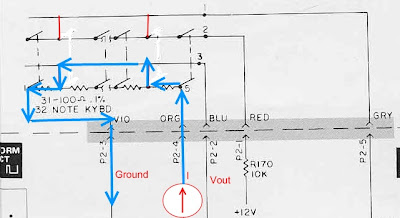
In a previous post I talked about how keyboard scanning works. The same method can be also used for switches that are not attached to keyboard keys, such as the
rainbow colored switches of the Roland Jupiter-8.
Here we see the schematics of Panel Boards G and E. The switches are shown with corresponding LEDs above them and, at the top, the function name, e.g. "TUNE", "A", "SPLIT." This should look very familiar; it's just like the keyboard scanning schematic. The output from the CPU (actually Panel Board A, more on that later) is fed to AG2-1,2,3,4 and AE2-1,2,3,4,5. As in keyboard scanning, the outputs cycle. First AG2-1 is high, everything else is low, then AG2-2 will be high, everything else will be low, and so on. During each cycle AG1-3,4,5,6,7,8 and AE1-1,2,3,4,5,6 will be read to see if any switches in a subset are currently pressed. The diodes are there for protection. So the only new thing is the LEDs, which are connected to the same outputs as the switches. How do they work?
The LEDs will illuminate when the diodes are forward biased. This occurs when a positive voltage is supplied from the Panel Board A outputs and current is being sunk from AG1-9,10,11,12,13,14 or AE1-7,8,9,10,11,12 back to Panel Board A. But we know that a positive voltage is only supplied a fraction of the time from the Panel A outputs. So the LEDs must only be "on" a fraction of the time. Whatever flicker is present must be imperceptible.
So the operation of the LED matrix is just like that of the switches except slightly backwards. The outputs are cycled through, corresponding to a subset of LEDs. Then, instead of a human pressing a switch and the CPU reading it, the CPU turns on an LED by sinking current and the human "reads" it. For example, suppose the "A" button LED on Panel Board G needs to be on. When AG2-2 is high, "6", "7", "8", "MANUAL", "A", or "B" can be turned on. Now the CPU has to sink current from AG1-10 to illuminate the "A." To understand this current sink, we'll take a look at Panel Board A.

First notice the LED Matrix in the upper right hand corner. The eight horizontal lines are the cycling outputs from Panel Board A. The six vertical lines are the current sinks for the LEDs going back to the "LED DATA LATCH." Here are a few interesting things to note:
- Boards E and G LED current sink lines are connected together to the same six LED lines.
- AE2-5 and AG2-1 are also tied together. There are really only eight outputs from Panel Board A to these switches/LEDs.
- The two boards are physically separate but effectively act as one.

Let's take a closer look at the current sink labelled "LED DATA LATCH." IC13 is a
D flip-flop. The inputs are on the bottom. Every rising edge clock (not the same as CPU clock) sets the outputs on top to the input logic states. Each flip-flop output drives a single transistor switch circuit. When the flip-flop output is high (5 V) AND the LED is biased with a positive voltage, the transistor will saturate, sinking current to put the collector near 0 V (0.05-0.2 V typically according to
Art of Electronics). This will turn on the LED. R40-45 are the current limiting resistors for the LEDs. The LED current will be about (5 - V
led)/100. Assuming Vled = 1.8 V, the current will be 32 mA. R46-51 have been designed with a resistance of 10k. I'll do some calculations to show why. The transistor base current is (5-V
be)/R
b = I
C/Beta. Assuming V
be = 0.7 V, I
C = .032 A, and Beta = 200, R
b comes out to 26k ohm. Using a lower resistance of 10k ensures there is ample current to put the transistor into saturation.
Let's back up and and figure out why there is a need for an LED DATA LATCH. Why do we need a flip-flop to store values? Notice on this block diagram the data bus is shared between the switches, LEDs, Numerical LED display latches, Interface board, and more. The LED DATA LATCH is needed in order to store values so the data bus can be used for other things. The flip-flop clock only triggers when the appropriate values are on the data bus.


